Would you like to make this site your homepage? It's fast and easy...
Yes, Please make this my home page!
Untitled Document
The Computer on a Chip
The
invention of the light bulb in 1879 symbolized the beginning of electronics.
Electronics then evolved into the use of vacuum tubes, then transistors, and
now integrated circuits. Today's microminiaturization of electronic circuitry
is continuing to have a profound effect on the way we live and work.
Current technology permits the placement of hundreds of thousands of transistors
and electronic switches on a single chip. Chips already fit into wristwatches
and credit cards, but electrical and computer engineers want them even smaller.
In electronics, smaller is better. The ENIAC, the first full-scale digital electronic
computer, weighed 50 tons and occupied an entire room. Today, a computer far
more powerful than the ENIAC can be fabricated within a single piece of silicon
the size of a child's fingernail.
Chip designers think in terms of nanoseconds (one billionth of a
second) and microns (one millionth of a meter). They want to pack as many circuit
elements as they can into the structure of a chip. High-density packing reduces
the time required for an electrical signal to travel from one circuit element
to the next—resulting in faster computers. Circuit lines on the initial
Intel processors (early 1980s) were 6.5 microns wide. Today's are less than
.5 microns. The latter holds 35 million transistors and is 550 times as powerful
as the initial one. By the turn of the century, researchers expect to break
the .2 micro barrier.
Chips are designed and manufactured to perform a particular function. One chip
might be a microprocessor for a personal computer. Another might be for primary
storage or the logic for a talking vending machine. Cellular telephones use
semiconductor memory chips.
The development of integrated circuits starts with a project review
team made up of representatives from design, manufacturing, and marketing. This
group works together to design a product the customer needs. Next, team members
go through prototype wafer manufacturing to resolve potential manufacturing
problems. Once a working prototype is produced, chips are manufactured in quantity
and sent to computer, peripheral, telecommunications, and other customers.
The manufacturing of integrated circuits involves a multistep process using
various photochemical etching and metallurgical techniques. This complex and
interesting process is illustrated here with photos, from silicon to the finished
product. The process is presented in five steps: design, fabrication, packaging,
testing, and installation.
DESIGN
1.
Using CAD for Chip Design Chip designers use computer-aided design (CAD) systems
to create the logic for individual circuits.
Although a chip can contain up to 30 layers, typically there are 10 to 20 patterned
layers of varying material, with each layer
performing a different purpose. In this multilayer circuit design, each layer
is color-coded so the designer can distinguish
between the various layers.
2. Creating a Mask
The
product designer's computerized drawing of each circuit layer is transformed
into a mask, or reticle, a glass or quartz plate with an opaque material (such
as chrome) formed to create the pattern. The number of layers dependson the
complexity of the chip's logic. The Pentium™ processor, for example, contains
20 layers. When all these unique layers are combined, they create the millions
of transistors and circuits that make up the architecture of the processor.
Photo courtesy of Micron Semiconductor, I
FABRICATION
3.
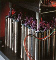
Creating Silicon Ingots Molten silicon is spun into cylindrical ingots. Because
silicon, the second most abundant substance, is used in the fabrication of integrated
circuits, chips are sometimes referred to as "intelligent grains of sand."
© M/A-COM, Inc.
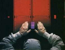
5. Wearing Bunny Suits
To
help keep a clean environment, workers wear semi-custom-fitted Gortex® suits.
They follow a hundred-step procedure when putting the suits on. Courtesy of
Intel Corporation
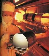
4. Cutting the Silicon Wafers
The
ingot is shaped and prepared prior to being cut into silicon wafers. Once the
wafers are cut, they are polished to a perfect finish. © M/A-COM, Inc.
6. Keeping a Cfean House
Clean
air confi'nuousCy flows from every pore of the ceiling and through the holes
in the floor into a filtering system at the manufacturing plant. A normal room
contains some 15 million dust particles per cubic foot, but a clean room contains
less than 1 dust particle per cubic foot. All of the air in a "clean room"
is replaced seven times every minute.
Portions of the micro chip manufacturing process are performed in yellow light
because the wafers are coated with a light-sensitive material called "photoresist"
before the next chip pattern is imprinted onto the surface of the silicon wafer.
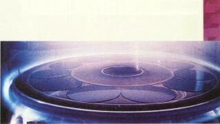
7. Coating the Wafers
Silicon
wafers that eventually will contain several hundred chips are placed in an oxygen
furnace at 1200 degrees Celsius. In the furnace each wafer is coated with other
minerals to create the physical properties needed to produce transistors and
electronic switches on the surface of the wafer
8. Etching the Wafer
A
photoresist is deposited onto the wafer surface creating a film-like substance
to accept the patterned image. The mask is placed over the wafer and both are
exposed to ultraviolet light. In this way the circuit pattern is transferred
onto the wafer. The photoresist is developed, washing away the unwanted resist
and leaving the exact image of the transferred pattern. Plasma (superhot gases)
technology is used to etch the circuit pattern permanently into the wafer. This
is one of several techniques used in the etching process. The wafer is returned
to the furnace and given another coating on which to etch another circuit layer.
The procedure is repeated for each circuit layer until the wafer is complete.
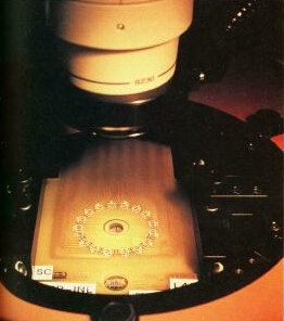
9. Tracking the Wafers
Fabrication
production control tracks wafers through the fabricating process and measures
layers at certain manufacturing stages to determine layer depth and chemical
structure. These measurements assess process accuracy and facilitate real-time
modifications.
10. Drilling the Wafers
It
takes only a second for this instrument to drill 1440 tiny holes in a wafer.
The holes enable the interconnection of the layers of circuits. Each layer must
be perfectly aligned (within a millionth of a meter) with the others.