Would you like to make this site your homepage? It's fast and easy...
Yes, Please make this my home page!
Untitled Document
PACKAGING
Removing
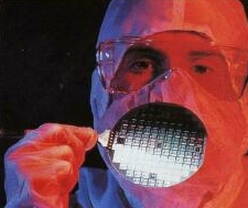
the Etched Wafers The result of the coating/etching process is a silicon wafer
that contains from 100 to 400 integrated circuits, each of which includes millions
of transistors.
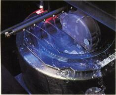
Mounting the Wafers
Each
wafer is vacuum mounted onto a metal-framed sticky film tape. The wafer and
metal frame are placed near the tape; then all three pieces are loaded into
a vacuum chamber. A vacuum forces the tape smoothly onto the back of the wafer
and metal frame.
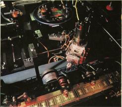
Dicing the Wafers
A
diamond-edged saw, with a thickness of a human hair, separates the wafer into
individual processors, known as die, in a process called dicing. Water spray
keeps the surface temperature low. After cutting, high-pressure water rinses
the wafer clean. In some situations, special lasers are used to cut the wafers.
Attaching the Die
Individual
die are attached to silver epoxy on the center area of a lead frame. Each die
is removed from the tape with needles plunging up from underneath to push the
die while a vacuum tip lifts the die from the tape. Lead frames are then heated
in an oven to cure the epoxy. The wafer map created in probe tells the die-attach
equipment which die to place on the lead frame.
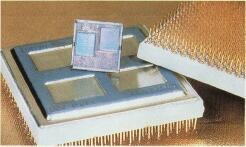
Packaging the Chips
The
chips are packaged in protective ceramic or metal carriers. The carriers have
standard-sized electrical pin connectors that allow the chip to be plugged conveniently
into circuit boards. Because the pins tend to corrode, the pin connectors are
the most vulnerable part of a computer system. To avoid corrosion and a bad
connection, the pins on some carriers are made of gold.